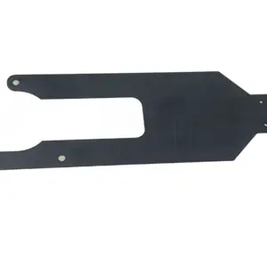

Wafer Transfer Robot Arm: The Core of Wafer Transfer Precision
The wafer transfer robot arm, also known as semiconductor robots arm or ceramic end effector, is an essential tool in the semiconductor manufacturing process. These devices ensure precise wafer handling, reducing contamination risks and improving production efficiency. From wafer cleaning to lithography, the robot arm guarantees accuracy and stability, making it indispensable for semiconductor manufacturers.
Why Ceramic Materials Are Ideal for Wafer Transfer Robot Arms
Ceramic materials, especially zirconia and high-purity alumina ceramics, are widely used in wafer transfer robot arms due to their outstanding technical properties. These materials provide the necessary strength, durability, and cleanliness required in semiconductor manufacturing.
Key Features of Alumina Ceramics
- High Purity and Antistatic Properties
Alumina ceramics with 99.7% purity and antistatic coating ensure optimal performance in cleanroom environments. - Mechanical Strength and Hardness
Alumina exhibits excellent wear resistance and dimensional stability, even under long-term use. - Low Thermal Expansion
This property ensures minimal deformation during temperature fluctuations. - Surface Quality
Advanced polishing and coating processes enhance flatness and reduce surface roughness, meeting stringent semiconductor manufacturing standards.
Superior Mechanical Performance
The wafer transfer robot arm achieves micron-level precision, thanks to its high rigidity and excellent bending resistance. This ensures stable and accurate wafer movement, even when handling wafers of various sizes and thicknesses.
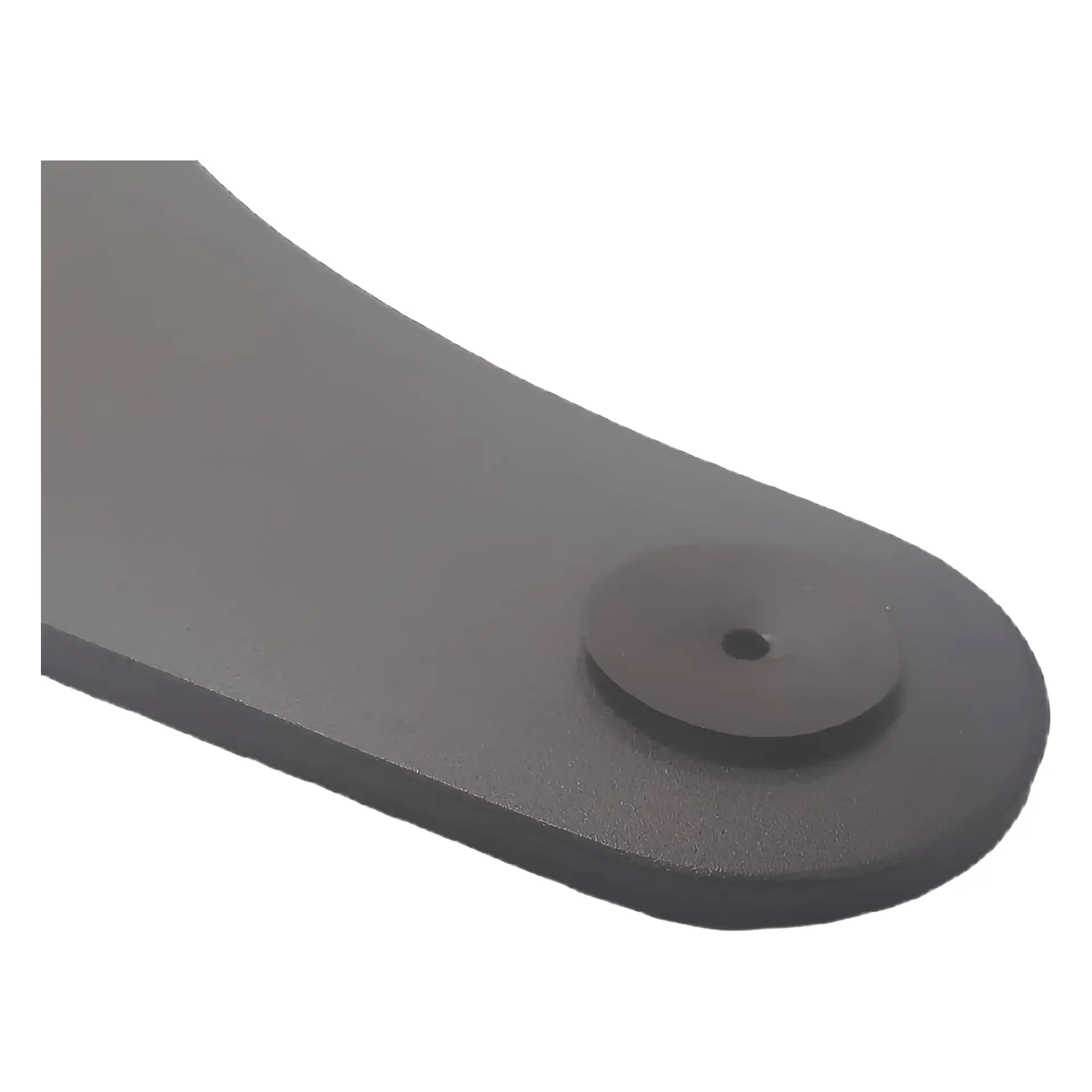
Advanced Surface Treatment Technology
- Precision Grinding and Polishing
Guarantees smooth surfaces for reduced particle generation. - Antistatic Coating
Prevents electrostatic discharge (ESD) damage. - Surface Roughness Control
Ensures optimal cleanliness and precision handling.
These technologies make ceramic wafer transfer robot arms highly reliable in cleanroom environments.
Applications in Semiconductor Manufacturing
Ceramic wafer transfer robot arms are ideal for handling wafers of different specifications, including 150mm to 300mm sizes. They adapt to various materials and thicknesses, ensuring precise positioning and alignment. Their stable performance supports processes like cleaning, etching, and lithography.
Manufacturing Processes
- Precision Molding and Sintering
Delivers high dimensional accuracy. - Surface Treatment
Enhances durability and cleanliness. - Assembly Precision
Ensures reliable performance during wafer handling.
Quality Control Standards
To meet semiconductor industry demands, ceramic wafer transfer robot arms undergo rigorous testing:
- Dimensional Accuracy
Ensures flatness and parallelism within 0.03mm. - Material Testing
Verifies mechanical and thermal properties. - Dynamic Performance
Confirms stability during operation.
Customization with LONGYI
LONGYI offers tailored solutions for wafer transfer robot arms. By providing 2D-PDF and 3D-STP files, customers can receive customized designs that meet specific requirements. Materials such as Alumina 99.7%, ESD-coated ceramics, and antistatic ceramics are available to suit diverse applications.